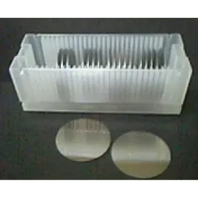
Ge(Germanium) Wafers
Ge(Germanium) Single Crystals and Wafers
Single crystal (Ge)Germanium Wafer
PWAM offers semiconductor materials,Ge(Germanium) Single Crystals and Wafers grown by VGF / LEC
General Properties of Germanium Wafer
|
General Properties Structure |
Cubic, a = 5.6754 Å |
||
|
Density: 5.765 g/cm3 |
|||
|
Melting Point: 937.4 oC |
|||
|
Thermal Conductivity: 640 |
|||
|
Crystal Growth Technology |
Czochralski |
||
|
Doping available |
Undoped |
Sb Doping |
Doping In or Ga |
|
Conductive Type |
/ |
N |
P |
|
Resistivity, ohm.cm |
>35 |
< 0.05 |
0.05 - 0.1 |
|
EPD |
< 5x10³/cm2 |
< 5x10³/cm2 |
< 5x10³/cm2 |
|
< 5x10²/cm2 |
< 5x10²/cm2 |
< 5x10²/cm2 |
|
Grades and Application of Germanium wafer
|
Electronic Grade |
Used for diodes and transistors, |
|||
|
Infrared or opitical Grade |
Used for IR optical window or disks,opitical components |
|||
|
Cell Grade |
||||
|
|
|
|
|
|
|
Standard Specs of Germanium Crystal and wafer |
||||
|
|
|
|
|
|
|
Crystal Orientation |
<111>,<100> and <110> ± 0.5o or custom orientation |
|||
|
Crystal boule as grown |
1" ~ 6" diameter x 200 mm Length |
|||
|
Standard blank as cut |
1"x 0.5mm |
2"x0.6mm |
4"x0.7mm |
5"&6"x0.8mm |
|
Standard Polished wafer(One/two sides polished) |
1"x 0.30 mm |
2"x0.5mm |
4"x0.5mm |
5"&6"x0.6mm |
|
Special size and orientation are available upon requested Wafers |
||||
|
|
|
|
|
|
|
|
||||
|
4 inch Ge wafer Specification |
|
|
|
|
|
Doping |
P |
|
|
|
|
Doping substances |
Ge-Ga |
|
|
|
|
Diameter |
100±0.25 mm |
|
|
|
|
Orientation |
(100) 9° off toward <111>+/-0.5 |
|
|
|
|
Off-orientation tilt angle |
N/A |
|
|
|
|
Primary Flat Orientation |
N/A |
|
|
|
|
Primary Flat Length |
32±1 |
mm |
|
|
|
Secondary Flat Orientation |
N/A |
|
|
|
|
Secondary Flat Length |
N/A |
mm |
|
|
|
cc |
(0.26-2.24)E18 |
/c.c |
|
|
|
Resistivity |
(0.74-2.81)E-2 |
ohm.cm |
|
|
|
Electron Mobility |
382-865 |
cm2/v.s. |
|
|
|
EPD |
<300 |
/cm2 |
|
|
|
Laser Mark |
N/A |
|
|
|
|
Thickness |
175±10 |
μm |
|
|
|
TTV |
<15 |
μm |
|
|
|
TIR |
N/A |
μm |
|
|
|
BOW |
<10 |
μm |
|
|
|
Warp |
<10 |
μm |
|
|
|
Front face |
Polished |
|
|
|
|
Back face |
Ground |
|
|
|
Germanium Wafer Process
Germanium blank or window are used in night vision and thermographic imaging solutions for commercial security, fire fighting and industrial monitoring equipment. Also, they are used as filters for analytical and measuring equipment, windows for remote temperature measurement, and mirrors for lasers.
Thin Germanium substrates are used in III-V triple-junction solar cells and for power Concentrated PV (CPV) systems.
Новости
Новые продукты от VivaTech
06.02.2018
VivaTech предлагает новые решения для применений в миллиметровом / THz диапазонах.
Новые продукты от A-Info
23.12.2016
AINFO предлагает к поставке новый волноводный ответвлитель и логопериодические антенны с простой и двойной поляризацией


